AES / SAM and Auger Depth Profiling
Principle
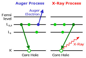
AES Auger Electron Spectroscopy and Scanning Electron Micrscopy SAM use a scanned focused high energy electron source to ionise electrons from the surface of a solid sample. An excited atom will then relax by electron shell to shell transition and the energy difference between the 2 shells must be released, emitted as either an X-ray or outer shell electron emission - the so called Auger electron. The kinetic energy of these Auger electrons are measured and are elementally characteristic. The low escape depth of Auger electrons means that AES analyses only the top few atomic layers of the sample material.
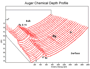
For analysis beyond the top 1-5nm an inert gas ion gun (normally Argon) can be used to sputter off the surface layers. Alternating sputtering and AES spectral acquisition permits chemical depth profiles to be obtained down to depths of about 1μm into the bulk.
Information Available from AES
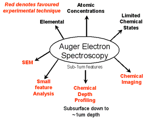
Main Features of the Laboratory's AES Capability
- Quantitative analysis of elements except hydrogen and helium
- Typical element detection limits are 0.1 atomic% from the top few nm
- SEM (scanning electron microscopy)
- Scanning Auger Microscopy (SAM) allows surface chemical maps to be collected with lateral resolutions better than 1μm.
- Chemical state information of certain elements (particularly Al, Mg, Si etc.) can be obtained
- Sputter depth profiling reveals chemical depth information
- Samples can be conductors and semiconductors. Analysis of insulators is more difficult but possible
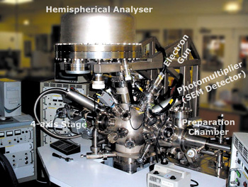
AES Instrument - VG Scientific ESCALAB 200-D
- 10keV LEG200 electron gun and photomultiplier for SEM
- 5 Channeltron Hemispherical Sector Analyser (HSA) for high and normal resolution Auger spectroscopy
- Computer controlled point and area spectroscopy linked to SEM image acquisition as well as Scanning Auger Microscopy chemical mapping capabilities www.iac.bris.ac.uk/scripts/softw1.htm
- EX05 inert gas ion gun for sample cleaning and Auger sputter depth profiling
- Optical camera for rough sample alignment
- Turbomolecular pumped fast entry air lock for rapid sample loading
- Multiple sample loading on extended stubs
- PC data acquisition and data processing system - www.casaxps.com
- 4 Axis stage with sample heating and cooling options
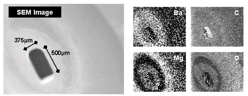
Typical Applications AES
- Metal component thermal oxidation or reduction process effectiveness (growth or removal of oxide or surface segregating materials)
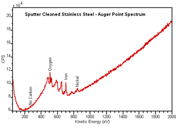
- Stainless steel laser welding difficulties solved by Auger depth profiling
- Characterisation of surface inhomogeneities
- Improvement of chemical cleaning or etching processes and analysis of drying stains
- Surface Oxide thickness in semiconductor processes - depth profiling
- Sputtered layer process chemical characterisation and depth profiling
- Wet chemical pitting corrosion studies
- Analysis of evaporated or deposited layers
Links to other sites
Thermo VG Scientific http://www.vgscientific.com - XPS and AES instrument Manufacturer.
Our site expert on XPS is Steve Jenkins.
Application Notes
