

SEM-EDX Analysis Services in Blackburn
Scanning Electron Microscopy (SEM) combined with energy dispersive X-ray (EDX) spectroscopy is one of the most powerful techniques available for examining the surface structure and chemistry of materials. A modern SEM / EDX instrument can produce 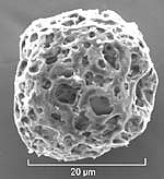 extremely high magnification images (up to 200000x) at high resolution (down to 2nm), while simultaneously generating localised chemical information for each area of the sample examined.
LPD Lab Services is an independent, UKAS-accredited analytical laboratory based in Blackburn, East Lancashire. We operate two SEM instruments and provide SEM-EDX analysis services to solve a wide range of product and processing problems for a diverse range of metals and materials, supporting clients across the UK.
Our laboratory has extensive experience in using SEM and EDX analysis across many industrial sectors, including electronics and semiconductors, pharmaceutical, petrochemicals, plastics and polymers, aerospace, automotive and medical devices, together with engineering, chemicals, materials and metallurgy.
How SEM-EDX Analysis Works
In the scanning electron microscope, a focused beam of electrons is scanned across the surface of the sample. Secondary electrons emitted from the surface are detected to form an image, revealing fine surface detail at magnifications up to 200000x and a resolution of 2nm. At the same time, the EDX detector identifies the elements present at each point by measuring the characteristic X-rays they emit.
Because both datasets are recorded from exactly the same area of the sample, our scientists can correlate structure with chemistry. That combination is what makes SEM-EDX analysis such a flexible tool for failure investigation: a single measurement can show what a feature looks like, where it is located, and what it is made of.
Typical SEM-EDX Analysis Applications
SEM-EDX analysis is applied to a very wide range of materials problems. Typical applications carried out by our laboratory include:
- Identification of metals and materials
- Particle contamination identification and elimination
- Classification of materials
- Product and process failure and defect analysis
- Examination of surface texture (including stereo imaging)
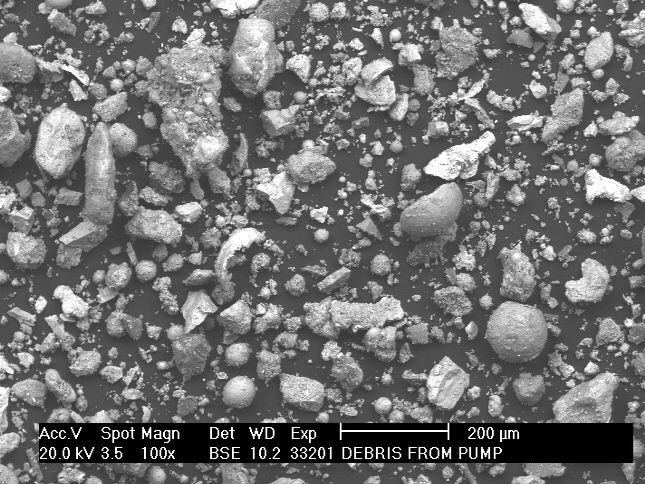
- SEM / EDX automated particle physical shape and size characterisation and EDX analysis
- Analysis and identification of surface and airborne contamination
- Powder morphology, particle size and analysis
- Cleaning problems, staining and chemical etching
- Welding and joining technology quality evaluation and failure investigation
- Paint and coating failure and delamination investigation
- Paint, Adhesive, Sealant and Gasket Filler Fingerprinting
- Identification and elimination of corrosion and oxidisation problems
- Contamination or surface stain investigation
- Structural analysis and microstructural analysis
- Reverse engineering of products and processes
- Braking system fault diagnosis
- Hazard investigation of exfoliants from a manufacturing process
- Source of fouling material in a returned product
- General hazard assessment of dust from storage areas
- Physical failure analysis of domestic water heaters and boilers
- Debris, particles, fibres and contaminant analysis in food and beverages
- Investigation of blistered coating on a yacht caused by sodium chloride crystals
- Investigation of cracked plastic components such as ABS and polycarbonate cracking associated with cleaning and sterilising agent use
- Stains on a car roof liner fabric traced to spherical mild steel particles from metalworking
- Root cause of wear debris in train and ship water pump systems to determine wearing parts
- Detection of zinc whiskers in PCBs in data centres
- Investigation of residues from a ship fire in a container
Particle Contamination and Failure Analysis by SEM-EDX
Many product and process problems are caused by a small quantity of foreign material: a particle, a fibre, a deposit, or a contaminant on a critical surface. SEM-EDX analysis provides the evidence needed to identify such material and trace its source. Each particle can be imaged at high magnification to establish its shape and size, and its elemental composition can then be measured directly by EDX without destroying the sample.
This combination of particle contamination identification and failure analysis is widely used in the electronics, pharmaceutical and medical device industries, where even a single foreign particle can lead to a defect, a batch failure, or a recall. For unknown materials, the same approach supports reverse engineering, the investigation of corrosion and oxidation, and the analysis of coatings and surface contamination.
Materials and Samples for SEM-EDX Analysis
A wide range of materials can be investigated by SEM-EDX analysis, including:
- Metals, glass and ceramics
- Semiconductors
- Plastics and polymers
- Powders, debris and dust
- Composite materials
- Fibres (textile, fabric, man-made, natural, carbon fibres, glass fibres, Kevlar)
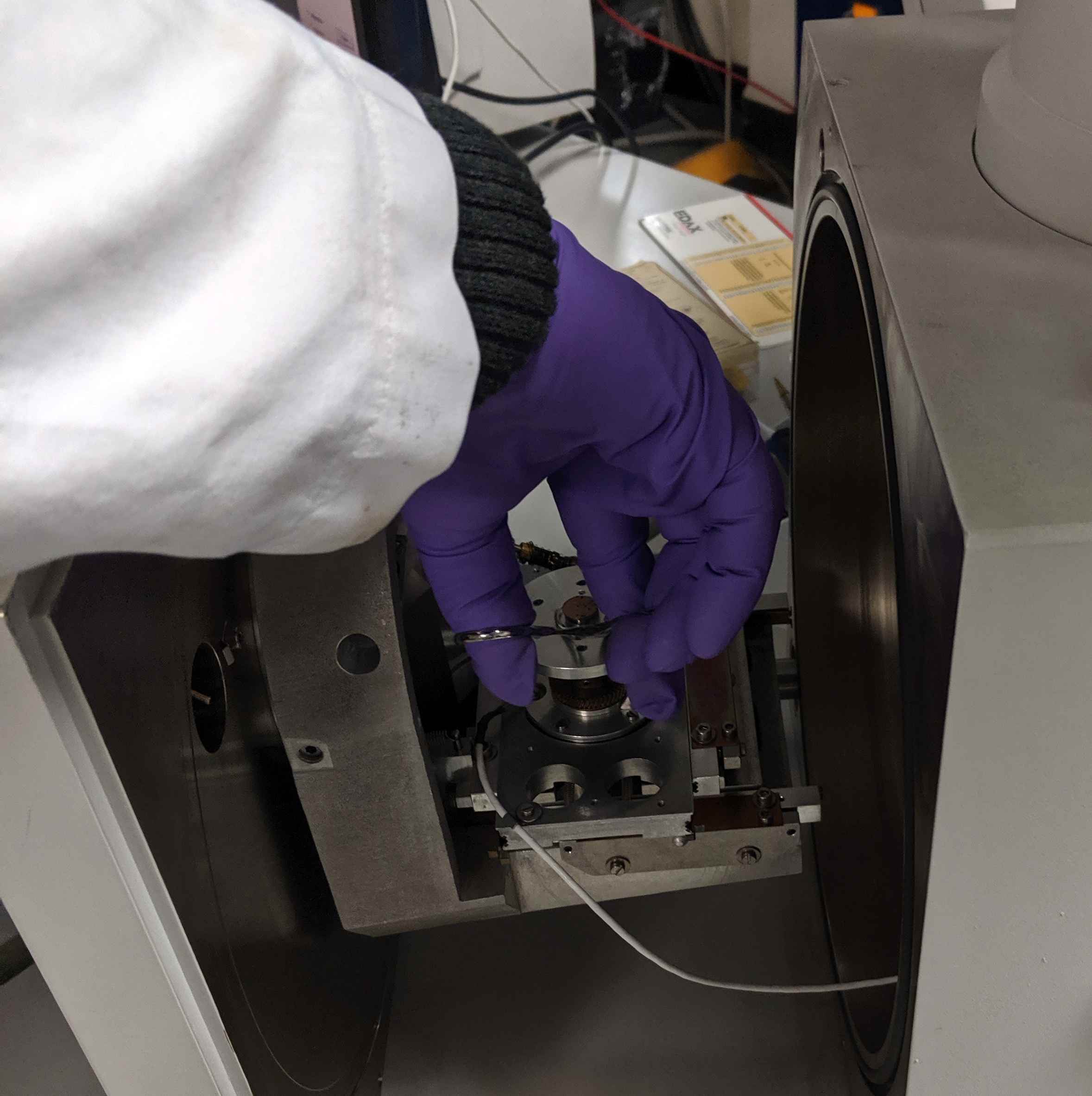
Samples are generally examined as received. Non-conductive materials, such as most polymers and ceramics, are typically given a thin conductive coating before imaging, as illustrated by the tungsten pellet case example below.
SEM-EDX Analysis Case Examples
The following examples illustrate the range of magnification, measurement and chemical analysis available from our SEM-EDX instruments.
Image Magnification, Measurement and Resolution
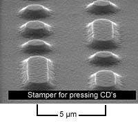 The first image shows the surface of a metal stamper used to imprint the information onto a compact disc during manufacture. It was taken at a magnification of 40,000x on the SEM, and illustrates the shape and structure of the individual bits of information.
The height, roughness and steepness of the sidewalls of the information are all critical to the manufacture of a good disc, as is the separation between adjacent tracks.
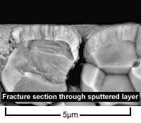 The second image is of a fracture section through a pellet made of tungsten powder that has been sintered and then sputter coated with an alloy of osmium and ruthenium.
The output from both the secondary electron and backscatter detectors has been mixed together on the SEM to highlight the sputtered layer on the surface of the pellet. This enables accurate measurement of the thickness of the sputtered layer and shows the growth structure through the layer. The thickness of the layer was measured at 640 nm.
Analysis of Thin Films by EDX
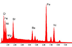 EDX analysis was carried out on a thin evaporated layer on top of a nickel / iron alloy.
The layer contained a mixture of barium, strontium and oxygen, with a small amount of magnesium. The thickness of the layer was calculated to be ~ 38 nm.
Frequently Asked Questions About SEM-EDX Analysis
What is SEM-EDX analysis used for?
SEM-EDX analysis is used to examine the surface structure and elemental composition of materials. Typical applications include particle contamination identification, product and process failure analysis, thin film measurement, powder morphology and particle size analysis, corrosion investigation, and reverse engineering of unknown materials and coatings.
What can a scanning electron microscope image show?
A scanning electron microscope produces high resolution images of a sample surface at magnifications up to 200000x and a resolution of 2nm. When combined with EDX, each feature in the image can also be chemically identified, so a single investigation can reveal both the shape and the composition of a contaminant particle, a defect or a thin film.
What types of sample can be examined by SEM-EDX analysis?
Most solid materials can be examined, including metals, glass and ceramics, semiconductors, plastics and polymers, powders, debris and dust, composite materials, and fibres such as textile, carbon, glass and Kevlar fibres. Samples are generally examined as received, and non-conductive materials may be given a thin conductive coating before imaging.
Is LPD Lab Services' SEM-EDX analysis UKAS accredited?
Yes. LPD Lab Services is an independent analytical laboratory based in Blackburn, East Lancashire, and is UKAS accredited. Our SEM-EDX analysis services are carried out by experienced analytical scientists supporting clients across the UK.
Request a Quote for SEM-EDX Analysis Services
If you would like to discuss your problem with us and find out how SEM-EDX analysis can help, please contact our laboratory in Blackburn, East Lancashire, today. Our site expert on SEM / EDX spectrometry is Keith Raper, and our team can advise on sample preparation, the most appropriate analysis, and indicative turnaround for your investigation.